Vertical integration of MEMS sensors on application-specific integrated circuits (ASICs)

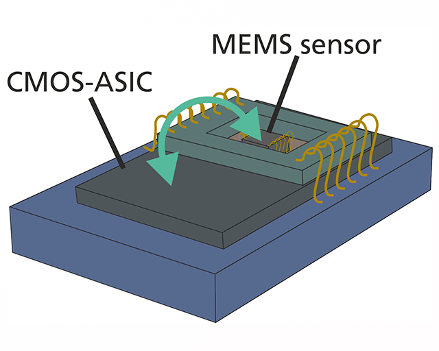
Nowadays, it is impossible to imagine our everyday life without consumer electronics products such as smartphones, tablets and smartwatches. Essential components of these products are the micro-electro-mechanical systems (MEMS) based sensors. While the dimensions of components, assemblies and devices are constantly being reduced; the size requirements of the wiring and encapsulation of the MEMS-ASIC components becomes a limiting factor for this size reduction.


In a joint project with the Fraunhofer institutes ILT and ISIT, the Fraunhofer IST has developed a deposition process for silicon which enables the direct deposition of silicon onto an application-specific integrated circuit (ASIC). As a result, the necessity of wiring between the MEMS and the ASIC component is completely eliminated, allowing for a significant reduction in overall component size.
Limitations of current solutions
More than 80 percent of all MEMS inertial sensors are fabricated in an epitaxial process by means of chemical vapor deposition (CVD), whereby deposition temperatures can exceed 1000 °C. Although there are possibilities for reducing the substrate temperature, significant limitations exist. A non-epitaxial thermal CVD process enables substrate temperatures to be reduced to ~650 °C; however, this leads to low deposition rates and amorphous, low-conductive, films. Advances in plasma-enhanced CVD (PECVD) have also achieved significant reductions in substrate temperatures, but result in a significant introduction of stresses into the resulting films, which in turn leads to deformation of fine MEMS structures.
The hot-wire solution
This is where hot-wire CVD (HWCVD) distinguishes itself. By depositing silicon at low substrate temperatures, a low-stress silicon film with large-area uniformity can be achieved whilst simultaneously achieving high deposition rates. In addition, high film conductivities can be achieved by adjusting the process parameters in such a way that the crystallinity of the films is increased.
The 7-chamber inline system at the Fraunhofer IST enables the deposition of silicon, silicon oxide and silicon nitride layers with industry-scale coating areas of more than 600 mm x 500 mm.
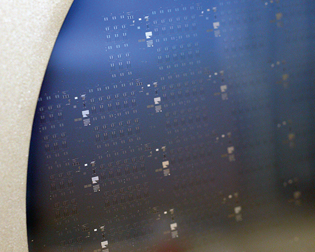
With the objective of direct MEMS-ASIC integration, the Fraunhofer IST has developed a novel silicon deposition process by means of HWCVD. This process enables the deposition of thick (> 10 µm), highly conductive (~0.1 Ωcm), nanocrystalline silicon films with the significant advantage of near-zero (< 10 MPa) film stresses. This is achieved whilst maintaining a low substrate temperature (< 420 °C), high deposition rates (> 1.8 nm/s) and very good scalability. The silicon layers were deposited on silicon wafers with NMOS (N-type metal-oxide-semiconductor) test structures, following which, MEMS structures were fabricated from these layers at the Fraunhofer ISIT.
The fundamental advantages of HWCVD silicon deposition are the resulting very low film stresses as well as the controllability of the film crystallinity. The performed work highlights an industrially relevant application of HWCVD technology in the further development of MEMS/ASIC sensor combinations. Vertical integration can provide a contribution towards further reducing the dimensions of electronic devices.
Outlook
This work describes an important advance in the application of HWCVD technology. A knowledge base for low-temperature processes has been established which, in addition to vertical MEMS-ASIC integration, opens up new possibilities for the deposition of MEMS-grade silicon on temperature-sensitive substrate materials.
This article is part of the Annual Report 2021.