Broadband beam splitter with low wavefront error

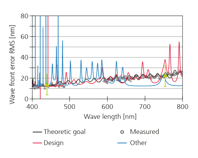
In many optical instruments so-called beam splitters are utilized. These are often used to separate individual spectral ranges in order to guide the light to the various spectrometers. With very high-quality instruments the wavefront error must be extremely small in order to minimize aberrations. Within the framework of a European Space Agency (ESA) project, the Fraunhofer IST has developed such a broadband beam splitter with very low wavefront error (20 nm rms).


The aim: coating of broadband beam splitters
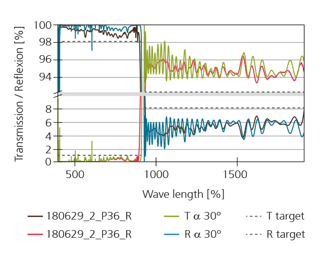
The aim of the project was to develop a beam splitter with a diameter of 120 mm which exhibits a high reflection of more than 98 percent in the spectral range of 400 to 900 nm at an angle of incidence of 30° and, simultaneously, a transmission of more than 92 percent in the NIR range of 920 to 2300 nm. In order to achieve this, a very high-quality optical coating was developed consisting of a dielectric layer stack, which was deposited with the help of the EOSS® (Enhanced Optical Sputtering System) sputtering facility.
Minimization of wavefront errors
Wavefront defects in optical coatings can have a number of causes. In order to minimize this error, a very high-quality substrate with a root mean square (RMS) error of 2 nm must first be utilized. A further source of errors are layer tensions, which can lead to bending of the substrate. Even for a substrate with a thickness of 12 mm, a non-compensated coating would lead to a distortion of more than 2 µm with a corresponding wavefront error. In the present case, an excellent compensation of coating stress could be achieved through a double-sided coating. Under certain circumstances, very large resonance-like wavefront errors can occur at certain wavelengths, which exceed the specifications many times over. In order to provide a solution for this situation, a completely new layer design was developed which is characterized by a very low wavefront error.
Production of the coating using the EOSS® facility
For the coating of the beam splitter, the EOSS® was utilized, with which high-precision optical interference filter systems can be produced. The total system consists of 150 layers and is 14.4 µm thick on both sides of the component. Through the optimization of the process, it was possible to significantly reduce the losses of the beam splitter. The deposition of the filter had to be performed with the highest precision as, due to the polarization splitting, a widening of the edge occurs for s- and p-polarized light. The layer design was created with a tolerance safety of less than 1 nm. In order to realize the smallest possible wavefront error, the deviation of the layer thickness distribution was reduced to a value of less than +/- 0.125 percent – worldwide a peak value.
This article is part of the annual report 2018.