High-resolution surface imaging using scanning electron microscopy: SEM

SEM image of a fracture edge with copper whiskers.
© Fraunhofer IST
SEM image of a fracture edge with copper whiskers.

Scanning electron microscopy in materials analysis

Scanning electron microscopy (SEM) allows the imaging of surfaces, fracture surfaces or transverse sections with high resolution (2 - 5 nm) and high depth of field. It is a versatile tool that permits movement through the magnification range by a factor of 20 to 200,000 times within seconds, quick changes from one sample to the next, and the imaging of non-conductive surfaces using vapor deposition. In combination with X-ray spectroscopy (EDX), SEM analysis is the ideal tool for damage analysis, as it combines microscopic visualization and chemical point analysis.

Special analysis methods on the scanning electron microscope (SEM)

  • Precise layer thickness determination in the nanometer to millimeter range by measurement of (cryo-)fractures or transverse sections
  • Imaging optimized for elemental or topographic contrast, through the use of different detectors (Inlens, SE, BSE)
  • Representation of the structure of materials through contrast optimization or etching of the surfaces
  • Analysis of microdefects through fabrication of local precision sections using Focused Ion Beam (FIB)
  • Production of lamellae for transmission imaging of the inner material structure

Cross-section through a wear-protection multilayer

Cross-section polish of a TiN/TiAlN multilayer with an ingrown defect.
© Fraunhofer IST

Cross-section of a TiN/TiAlN multilayer with ingrown defect. The contrast between the layers arises from the different average atomic number of the TiN layers (light) and the TiAlN layers (darker). The WC hard metal substrate appears particularly bright.

Fracture edge of a DLC layer

REM breaking edge DLC film. DLC film with various intermediate layers.
© Fraunhofer IST

DLC layer with various metallic intermediate layers. The intermediate layers show distinct columnar growth structures, while the DLC layer is amorphous and structureless.

Imaging of nanofibers

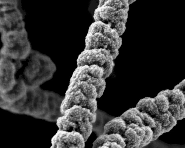
Hochauflösende Abbildung von beschichteten Nanofasern zeigt die Faserdurchmesser von ca. 300 nm und die ca. 10 nm großen Körner der metallischen Beschichtung.
© Fraunhofer IST

High-resolution image of coated nanofibers showing the fiber diameters of around 300nm, and the grains of the metallic coating, which are around 10nm in size.

Micro grinding pencil with CVD diamond coating imaged under a scanning electron microscope (SEM)

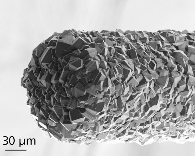
CVD diamond coated micro grinding pencil.
© Fraunhofer IST
CVD diamond coated micro grinding pencil.
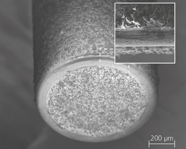
Conventional diamond milling bit with electroplated bond (D15) following machining of zirconia ceramic, with the abrasive coating completely worn away at the tip.
© Fraunhofer IST
Conventional diamond milling bit with electroplated bond (D15) following machining of zirconia ceramic, with the abrasive coating completely worn away at the tip.
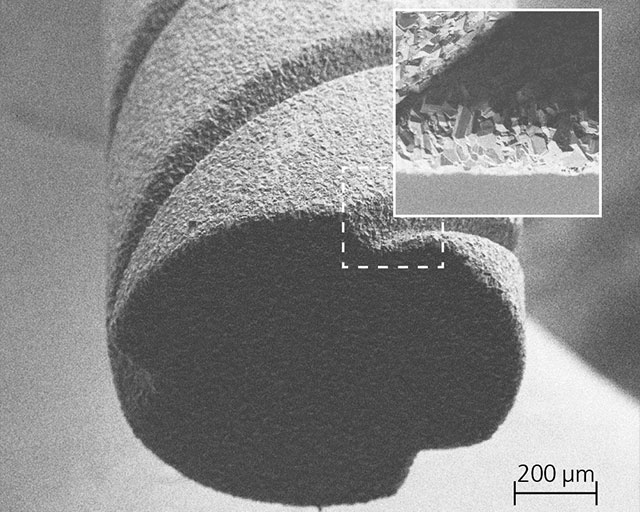
CVD diamond milling bit with ground spiral grooves following machining of zirconia ceramic
© Fraunhofer IST
CVD diamond milling bit with ground spiral grooves following machining of zirconia ceramic

Our focus and expertise in high-resolution surface imaging using scanning electron microscopy


Microscopy and surface measurement

Focused Ion Beam

Production of local precision cross-sections allows a view below the surface