Silicon layers for heterostructure solar cells

For decades, silicon has been used as a semiconductor and is therefore an important component in the photovoltaic industry. Among the solar cells based on crystalline silicon (c-Si), silicon heterostructure solar cells (silicon heterojunction, SHJ) distinguish themselves through their particularly high efficiency rates of more than 26 percent. Hot-wire chemical vapor deposition (HWCVD) presents a promising technology for the cost-effective deposition of low-defect silicon layers. For this reason, the Fraunhofer IST is utilizing the process in order to investigate its suitability for the manufacture of highly efficient SHJ solar cells, in particular for applications within the automotive sector.


The structure of SHJ solar cells
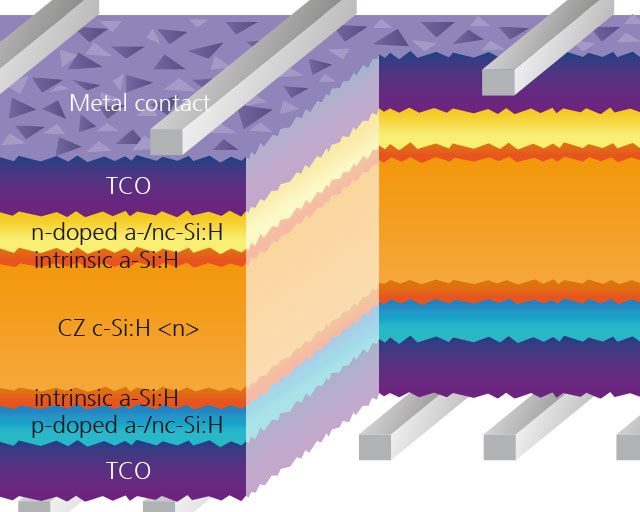
In SHJ solar cells, crystalline Si wafers serve as absorbers in which sunlight is converted into free charge carriers. Decisive for the achievement of high efficiency rates in these solar cells is that the charge carriers, during their passage to the contacts, do not recombine at defects on the wafer surfaces which act as recombination centers. For the saturation of surface defects, extremely thin passivation layers made from amorphous silicon (a-Si:H) are applied to both sides of the wafer, followed by the p- or n-doped Si layers, a transparent conductive oxide layer (TCO) and, finally, the metallic contacts (see adjacent Figure above).
Advantages of hot-wire-activated gas-phase deposition
Within the framework of a project funded by the BMWi, the HWCVD process is used instead of the plasma-enhanced chemical vapor deposition (PECVD) for the production of intrinsic and doped silicon layers. With HWCVD, the process gas mixtures are activated by resistively heated metal wires. The layer formation takes place exclusively through radicals formed thereby in complete absence of high-energy particles. As HWCVD deposition therefore takes place without particle bombardment, the process is particularly suitable for the gentle production of low-defect coatings, which are expected to exhibit exceptionally good passivation properties. A further advantage is that through HWCVD processes, it was possible to achieve a high process gas exploitation of more than 80 percent and, therefore, also higher deposition rates of more than 2 nm/s. This results in considerable cost advantages compared to PECVD processes.
Deposition of silicon layer stacks
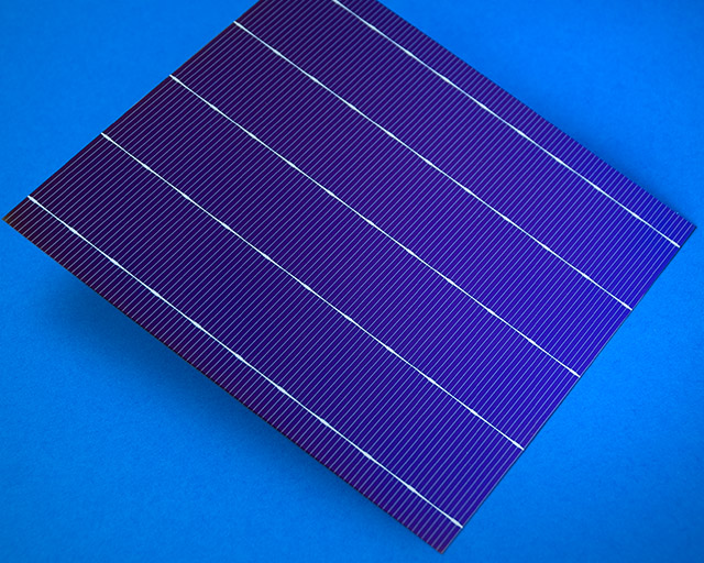
The silicon layers were deposited in a large-area HWCVD inline coating system developed by the Fraunhofer IST (see Figure above), which has three coating chambers with areas of up to 500 x 600 mm². As shown in adjacent Figure below, four solar wafers with a format of 156 x 156 mm² can be coated simultaneously. The process conditions were optimized for layer thicknesses of 10 to 20 nm. On textured wafers, charge carrier lifetimes of up to 5 ms were achieved. As the basis for the production of SHJ cells, passivation layers with a thickness of 6 nm and carrier lifetimes of around 1 ms were first utilized. The production of the n- and p-doped silicon layers was carried out through the addition of the doping gases phosphine (PH3) and diborane (B2H6). The conductivity of the doped layers was pre-optimized through the addition of hydrogen (H2), whereby the layers became nanocrystalline.
Results
The stacks of intrinsic a-Si:H passivation layers produced at the Fraunhofer IST from pure SiH4 gas and doped layers with differing conductivities and layer thicknesses were further processed by the project partners to form complete solar cells, and the component properties were investigated by means of their current-voltage characteristic curves. With the layer stacks tested to date, cell efficiency rates of 19.4 percent have already been achieved. Through further optimization of the layer system, the efficiency rates should be significantly improved by the end of the project.
The project
The work presented here was carried out within the framework of the project “Prozess- und Anlagentechnologie zur kostengünstigen und ressourcenschonenden Herstellung von Silizium-Heterostruktursolarzellen mit hohem Wirkungsgrad” (process and plant technology for the cost-effective and resource-saving manufacture of silicon heterostructure solar cells with high efficiency rates, “PATOS”), which is funded by the German Federal Ministry for Economic Affairs and Energy (BMWi) and which will run from 1st September 2016 to 31st August 2019.