Very-high resolution 3-dimensional surface imaging: AFM

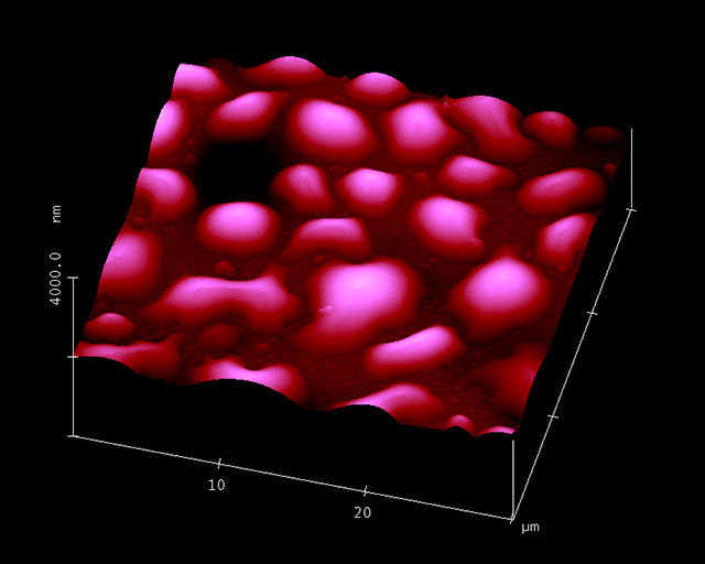
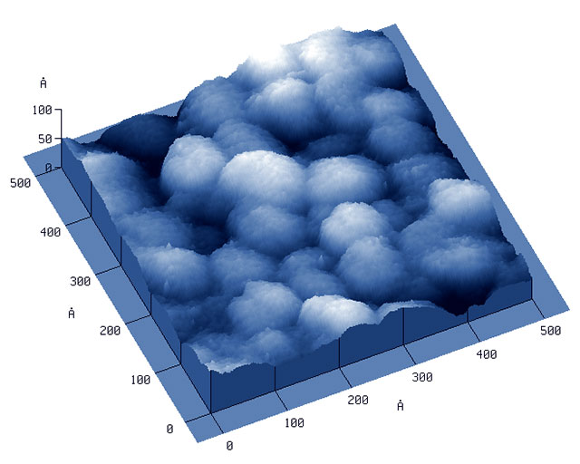
3D image of a polycrystalline diamond layer.
© Fraunhofer IST
3D image of a polycrystalline diamond layer.

Atomic Force Microscopy (AFM)

The atomic force microscope and the scanning tunneling microscope (AFM/STM) are suitable for images with particularly high resolution. The surface is scanned by means of an ultra-fine tip, with minimal force, generating a 3D image of the surface. Lateral resolutions of 1-10 nm and vertical resolutions of less than 1 nm are achieved. Monolayer samples can be resolved. The atomic force microscope (AFM) is particularly suitable for characterizing extremely smooth surfaces. Friction microscopy or modulation techniques can also be used to show material contrasts.

Quantitative evaluation

The advantage of Atomic Force Microscopy (AFM) is that it provides not only a "photo" of the surface, but a complete three-dimensional data set of the surface topography. A great deal of quantitative information can be obtained from this:

  • Roughness
  • Step heights and widths
  • Pitch angle
  • Grain sizes
  • Skewness and kurtosis
  • Power spectral density and more

The data can also be made available as a 3D data set to the customer for their own evaluations.
STM image of a metal DLC layer

Nanocrystal platinum particles in an amorphous carbon matrix.
© Fraunhofer IST

The figure shows nanocrystalline platinum particles in an amorphous carbon matrix. The platinum particles have a diameter of just a few nanometers, but appear somewhat enlarged in the image due to folding with the geometry of the scanning tip.

Polymer surface

AFM tapping mode image of a polymer surface.
© Fraunhofer IST

AFM-tapping-mode-image of a polymer surface. Tapping mode is a very low-impact scanning method, with which even soft materials such as polymers can be imaged without damage.

Microchip surface

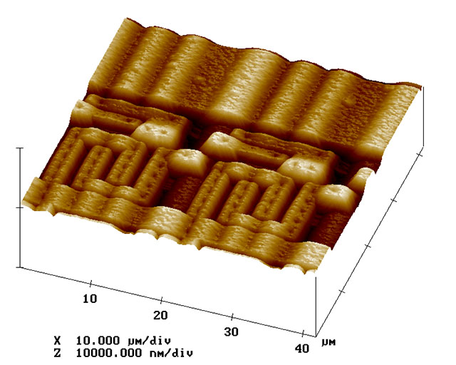
3D image of the surface of an electronic microchip.
© Fraunhofer IST
3D image of the surface of an electronic microchip.
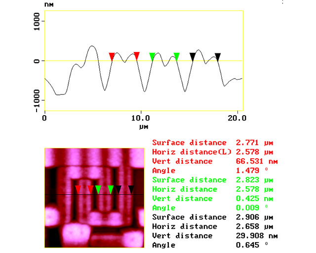
3D images of the surface of an electronic microchip and measurement of the structure sizes.
© Fraunhofer IST
3D images of the surface of an electronic microchip and measurement of the structure sizes.

Glass

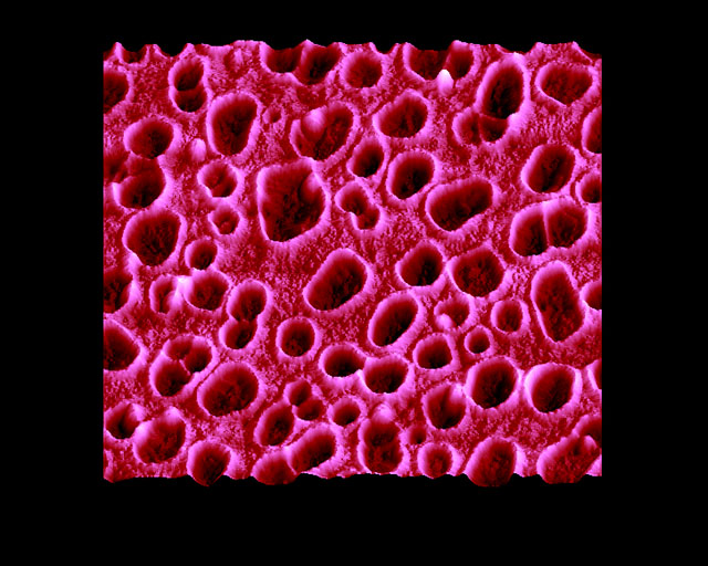
Pitting in corroded glass surface.
© Fraunhofer IST
Pitting in corroded glass surface.

Further information on our expertise in atomic force microscopy (AFM)


Chemical, mechanical and thermal surface treatment

Configuration of the surface topography


From research

Anti-adhesive systems for plastics molding


Reference project

Optical coatings with low residual stress


Reference project

Parabolic mirrors for space – with lightweight CFRP