Atmospheric pressure plasma processes

In order to effectively modify, functionalize or purify surfaces, atmospheric-pressure plasma processes are successfully applied in many sectors of industry. In addition to medical technology, examples include microsystems technology, the packaging and capital goods industries, the electronics industry, the automotive sector and the aerospace industry. At the Fraunhofer IST, we develop application-specific plasma sources and coating systems which cover a wide range of coating functions and which can therefore not only be deployed in a targeted manner for the cleaning, functionalization or coating of a wide variety of materials and geometries but can also be integrated into existing process chains. In addition to conventional organosilicon layer formers, bio-based systems are also increasingly being used for this purpose.
Industrially suitable, implementable processes
Coating procedures that dispense with wet-chemical processes or downstream drying processes possess great potential for industrial applications. In order to replace established processes, alternative processes must have attained a sufficient degree of maturity, offer added value and, ideally, conserve resources. Atmospheric-pressure plasma processes offer numerous advantages here.
Sustainable bio-based coating systems
The functionality of surfaces depends significantly on the chemical composition of the surface. This is indeed the case in established atmospheric-pressure plasma processes. If layer formers, so-called precursors, are then added to the plasma, thin layers can be deposited by means of APPP. Increasingly, bio-based systems are hereby being used which, due to their chemical properties, have a specific functionality, e. g. hydrophobic, dirt-repellent or antimicrobial properties. In many applications, examples from nature serve as models.
Adapted plasma processes for specific requirements
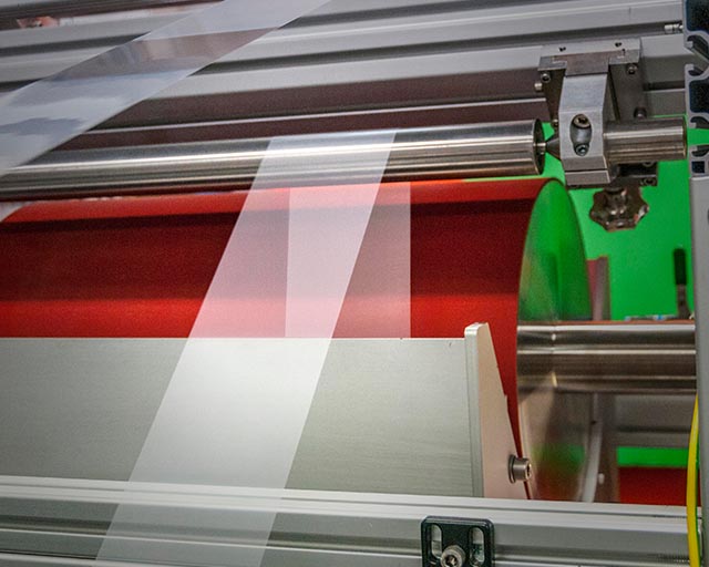
In contrast to highly volatile, conventional organosilicon layer formers, it is necessary to adapt the coating systems to such higher-molecular-weight starting materials. This is where our expertise really comes into play. Not only large-volume roll-to-roll processes requiring linear coating systems are taken into consideration, but also the robot-guided deployment of plasma jets or spatially-resolved coating by means of plasma printing. Adapted plasma processes and coating systems then provide the basis for the deposition of sustainable coating systems.
”Our expertise in plasma-source development, in combination with adapted coating technologies and flexible production processes – with a focus on sustainably functional surfaces – provides an important building block for the circular economy.”
Dr. Kristina Lachmann, Group Manager


