Atomic Layer Deposition ALD

For the production of high-tech materials, components and products for which ultra-thin layers with an extremely uniform and defined layer thickness are required, including on large and structured surfaces, atomic layer deposition is often the technology of choice. With our hybrid spatial ALD facility, atomic layer deposition processes can be combined in high rate with other coating and activation processes. This cutting-edge technology in the field of modern manufacturing processes and automation enables us to deposit thin layers homogeneously and with high conformity on the most varied components.
Coating and process development for the deposition of conformal and uniform coating systems
Atomic layer deposition is a modified process of chemical vapor deposition. The characteristics of the process are two successive self-limiting surface reactions, so that extremely thin, low-defect and extremely homogeneous layers can be deposited. A key advantage is the precise control of layer thickness and material composition for three-dimensional, complex geometric or structured substrates, resulting in highly conformal and uniform layers.
Your partner for innovative coating solutions
The Fraunhofer IST offers customers from industry and research application-specific and flexible solutions. Our services in the field of conformal coatings range from process development for thermal ALD coating systems to the development of customized functional coatings on particle materials and complex geometric substrates for optics, applications in medical and pharmaceutical industries as well as the energy materials development.
Atomic layer deposition for medical-technology applications
Medical-technology innovations from small and medium-sized companies often fail due to the implementation of special processes which are necessary for the manufacturing of the medical product, and consequently do not achieve the transfer from basic research to the market. In contrast, expensive machines in universities are not sufficiently utilized. The platform “Translational Manufacturing Platform Medical Innovation” optimizes the technology and knowledge transfer of special processes based on atomic layer deposition at the Fraunhofer IST. In this context, we offer, on the basis of this coating technology, the development and optimization of nanometer-thick diffusion barrier coatings for e. g. implants with deep-lying micro undercuts or vertical material interfaces.
Compliant coatings and functionalizations for applications in the energy sector
Nanomaterials are considered to be a pathway towards the implementation of renewable energy technologies – from energy generation through to energy storage. In the manufacturing of these nanomaterials and in their modification, functionalization and stabilization many challenges arise. The extensive range of ALD process variants at the Fraunhofer IST enable rapid target and customer-oriented implementation of layer and process development for a wide variety of substrate materials, geometries and dosage forms.
Beneq TFS 500
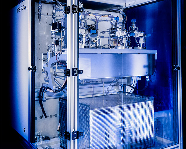
The Beneq TFS 500 is a coating system based on thermal atomic layer deposition for research and development and batch production for the production of homogeneous and uniform single layers as well as nanolaminate systems. The focus is on the deposition of metal oxides (e.g. Al2O3, TiO2, ZnO, SnO2, Nb2O5, SiO2) for application as optical functional layers, barrier layers, battery material functionalization, particle and textile coatings.
Specifications / technical data
- Thermal atomic layer deposition
- Batch coater (cross flow & stop flow for 2D/3D, forced flow fluidized bed for particles)
- 3D-lock and 2D-loadlock
- Substrate materials: wafers, glass, plastics, metals, textiles, particles
- Single wafer: ø200 ×10 mm
- 3D-batch (multiwafer): ø210 × 170 mm
- Particle coating: ø80 × 50 mm (~ 100 cm3), particle size > 10 µm
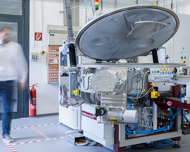
FHR Star 400x300 SALD
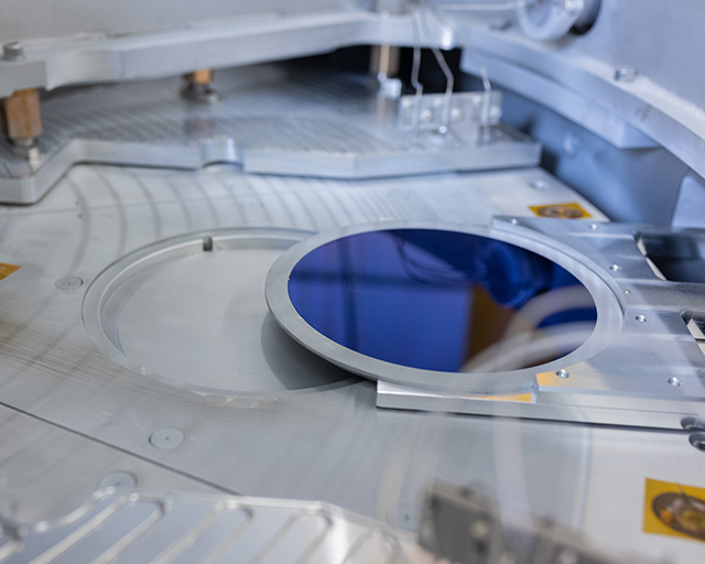
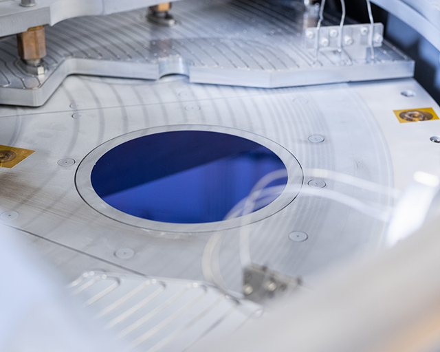
The FHR Star 400x300 SALD coating system is based on thermal local atomic layer deposition for high throughput coating for the deposition of homogeneous and uniform single layers as well as nanolaminate systems. The focus is on the deposition of metal oxides for application as optical functional layers, barrier layers, energy material functionalization and textile coatings. The flexible design allows the integration of different coating and activation options within a dedicated hybrid area as well as within the precursor zones.
Specifications / technical data
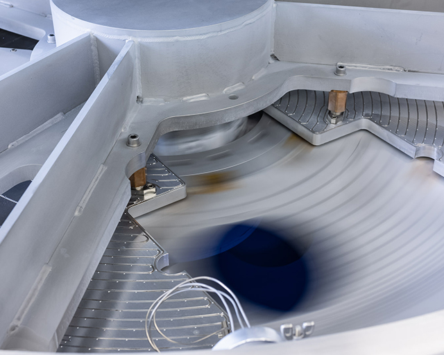
- Rotary table apparatus for thermal local atomic layer deposition
- 100 rpm (Al2O3: 10 nm/min)
- Substrate materials: wafers, glass, plastics, metals, textiles
- 4x 2D substrates: ø 200 mm
- 2x 3D substrates: 400 x 300 mm
- Maximum substrate thickness: 10 mm
- Hybrid zone for the integration of various coating and activation options
- Modular and flexible apparatus design and process adaptation
”The technological innovations and application possibilities of atomic layer deposition are developing rapidly. Our goal is to transfer these swiftly and efficiently to our customers.”
Dr.-Ing. Tobias Graumann, Team Manager
