Materials for sustainable tandem solar cells with maximum conversion efficiency
Fraunhofer Lighthouse Project


Challenge
In order for photovoltaics to be able to reliably ensure the power supply – e.g. for energy-autonomous buildings, electric cars or other products – at an acceptable cost, solar cells are necessary which are as efficient as possible and which require correspondingly less material and surface area than conventional modules. For physical reasons, however, the efficiency of established silicon solar cells cannot be increased arbitrarily.
Solution
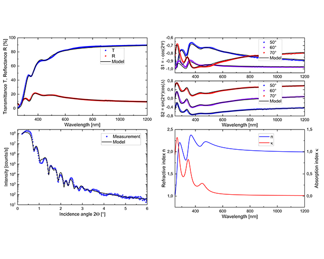
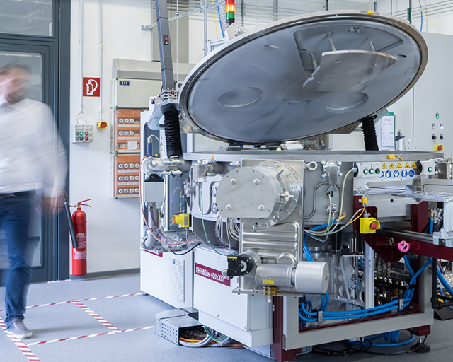
In a joint project, 5 Fraunhofer institutes are therefore working on the development of perovskite silicon tandem solar cells with which efficiencies of more than 35 percent can be achieved. Within this context, both equipment technology and manufacturing processes are being further developed and adapted. The focus here is on the production of large-area selective charge-carrier layers, buffer and passivation layers, and transparent conductive oxides (TCOs) by means of sputtering processes. For the development of the electron contact system, a novel high-rate SALD hybrid facility is being utilized. Within the framework of the project, indium-based TCOs were optimized and the processes were transferred to a large-area sputtering facility. In addition, a novel hybrid system setup consisting of atomic layer deposition and evaporator unit was assembled and the first combination layers were produced. Furthermore, optical models for the determination of dispersion data were developed in order to simulate cell performance.
Added value
The Fraunhofer IST has amassed extensive experience in the field of thin-film and silicon technology for photovoltaics. As a result, it is possible, amongst other things, to ensure that the various layers are adapted both electronically and optically – i.e. with low absorption – to the absorbers; in this case, silicon and perovskite. In addition to its expertise in layer and process development, the Fraunhofer IST offers customer-specific services in the field of sustainability management and life cycle engineering.

